Machining for the Semiconductor Industry: Types of Machining, Large to Small Parts, Major Japanese Companies, Machine Tools and Cutting Tools, New Technologies, How to Enter
After dimensions come dirt, gas and leaks. If you can handle the steps before and after cutting too, that's a real strength!

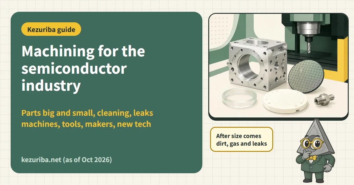
Investment in semiconductor manufacturing equipment keeps hitting record highs, and sales by Japanese equipment makers are expected to exceed ¥6.5 trillion in FY2026. Inside that equipment are aluminum vacuum chambers, electropolished stainless steel gas components, and precision parts in ceramics and quartz: a mass of machined parts. This article covers what kinds of machining there are, parts from large to small and the accuracy they require, key points for each material, the cleanliness and leak tightness required beyond dimensions, the machine tools and cutting tools used, the major Japanese companies, new technologies seen in research papers, and entry routes, the order of steps and the hurdles, based on maker documents, SEMI standards, patents, papers from J-STAGE and elsewhere, and public materials from industry associations and companies (as of October 2026).
Why look at semiconductors now
According to SEMI, worldwide sales of semiconductor manufacturing equipment reached a record $135.1 billion (up 15% year on year) in 2025. The forecast for 2026 is $165.9 billion (up 23.2%), and sales are expected to grow to $229.5 billion in 2028[1][2]. Sales in April–June 2026 were $40.5 billion, a record for the second quarter in a row[3]. Investment in leading-edge logic for AI servers and in memory, led by HBM, is driving the growth[4].
Sales by Japanese equipment makers (what Japanese companies sold at home and abroad) will rise, according to the July 2026 forecast of the Semiconductor Equipment Association of Japan (SEAJ), from the FY2025 actual of ¥5.1986 trillion to ¥6.5502 trillion (up 26%) in FY2026, ¥7.4017 trillion in FY2027 and ¥7.7718 trillion in FY2028. Demand from fabs in Japan (the Japanese market) is also expected to exceed ¥2 trillion for the first time in FY2028[4].
In Japan, the government has decided to subsidize TSMC's Kumamoto fabs (JASM) with up to ¥476 billion for Fab 1 and up to ¥732 billion for Fab 2[7], and Rapidus in Chitose, Hokkaido, plans to start volume production of 2nm logic in the second half of FY2027[8][9]. The government has set out a framework to draw over ¥50 trillion in public and private investment with more than ¥10 trillion in public support by FY2030[6]. In Kumamoto, 68 companies had announced new sites or expansions as of September 2024[7], and 62 companies had decided on sites in and around Chitose as of June 2026[9].
| Equipment destination, 2025 | Sales | YoY |
|---|---|---|
| China | $49.3 billion | −0.5% |
| Taiwan | $31.5 billion | +90% |
| Korea | $25.8 billion | +26% |
| North America | $10.9 billion | −20% |
| Japan | $9.5 billion | +22% |
| Europe | $2.9 billion | −41% |
SEMI data by region (where the equipment was delivered)[1]. China, Taiwan and Korea together account for 79% of the total. Demand from fabs in Japan (¥1.4395 trillion in FY2025) is just under 30% of the sales of Japanese-made equipment[4], so parts machining work in Japan also depends on fab investment across Asia.
But the swings are bigIn 2009, after the Lehman shock, worldwide equipment sales nearly halved from the year before (down about 46%; January–March was down 71% year on year), and sales to Japan fell about 68%[5]. Demand from fabs in Japan fell 29.5% in FY2019[4]. The forecasts themselves move too: SEAJ's FY2026 forecast rose by more than ¥1 trillion in the six months from January to July[4]. The more a company adds equipment in today's boom, the more it needs to plan its cash flow for the down years in advance.
Semiconductor machining falls into 3 worlds
When people hear "semiconductor processing," they tend to think of microfabrication on the wafer (lithography, etching), but that is work done by chemistry and light inside the equipment. Lathes, machining centers and grinders come in broadly in the following 3 areas.
| World | What is machined | Main materials | Nature of the work |
|---|---|---|---|
| ① Equipment parts | Vacuum chambers, bases and frames, stages, gate valves, gas blocks and fittings, transfer robot parts | Aluminum (A5052, A6061), stainless steel (SUS316L), welded steel structures | Made to the equipment maker's drawings. Sensitive to business cycles, but high volume |
| ② Process parts (consumables) | Showerheads (electrode plates), focus rings, electrostatic chucks, quartz tubes and boats | Silicon, SiC, quartz, and ceramics such as alumina and AlN | Eroded by plasma or heat, so replaced regularly. Orders come every month as long as the fabs run. There is also refurbishment (remanufacturing) work[35] |
| ③ The wafers and chips themselves | Ingot slicing, grinding, lapping and polishing, backgrinding, dicing | Silicon, SiC, GaN, glass | A world of dedicated equipment and tools. Machining companies are usually involved from the side of equipment, tools and fixtures |
Lathe and machining-center shops usually find ① the easiest to enter; companies strong in grinding and in hard, brittle materials fit ②; ③ is mainly the domain of equipment, tool and grinding wheel makers and research institutes. This article focuses on ① and ②, and for ③ introduces what is happening and the new technologies.
From large to small: sizes and requirements by part
| Part | Materials | Example size | Requirements (examples) | Main machines |
|---|---|---|---|---|
| Base & frame | Welded steel structure | Several m | Control welding distortion and machine the mounting faces in one setup. Integrated fabrication → machining → painting → assembly[41] | 5-face machine (e.g. X 6,700 mm class), horizontal boring mill |
| Vacuum chamber | A5052, A6061, SUS316L | From φ500–600 mm internal parts up to 2.7 m-class lengths[42][40] | e.g. geometric tolerances of 0.01 mm or less, Ra 0.2–0.4 µm[42]. Scratches and dents on seal faces cause vacuum leaks | 5-axis and double-column machining centers, large anodizing tanks |
| Gate valve | Stainless steel, aluminum | 50 kg each at the 250 mm bore class[31] | Specs such as a body leak rate below 5×10⁻¹⁰ mbar·L/s[31] | Machining, welding, leak testing |
| Gas blocks & fittings | SUS316L (double-melted) | A few mm to 100-odd mm | Wetted surface Ra 0.13 µm by electropolishing; surface Cr/Fe ratio of 2.0 or more, etc. confirmed by analysis[25] | CNC automatic lathes, multitasking machines, electropolishing, TIG welding |
| Showerhead (electrode plate) | Aluminum, silicon, SiC | Plates over φ300 mm. Some designs have tens of thousands of φ0.1–0.6 mm holes[34] | Consistent hole diameters and positions; no burrs or contamination inside the holes | Small drills on high-speed machining centers, small-hole EDM, laser |
| Focus ring | Si, CVD-SiC, quartz | e.g. OD φ360–380 mm[35] | Replaced when eroded. SiC rings can also be rebuilt by redepositing material[35] | Surface and cylindrical grinding, diamond tools |
| Electrostatic chucks & stages | Alumina, AlN | φ300–500 mm | e.g. flatness of 1 µm on φ500 mm alumina[37] | Surface grinding, lapping, ultrasonic machining |
| Quartz tubes & boats | Quartz glass | Up to 1 m class in length | Minimum hole φ0.3 mm (machining, laser), through to welding and annealing[36] | Machining, laser, flame working |
| Pins, screws & small parts | Ceramics, resin, SUS | From a few mm | High quantities, but the same cleanliness requirements as large parts | Automatic lathes, grinding |
Values are from maker documents, patents and machining examples, and vary by equipment and customer.
For large parts, the limit is the tank and the room, not the machineEven if you can machine a large chamber, you can't deliver it unless it fits into the anodizing or thermal-spray tanks, the washer, the cleanroom and the helium leak test room. One benchmark: there are companies that can process parts up to 2.7 m long and 400 kg[40]. For processes you don't have in-house, propose them as a package with a processing partner.
Key points by material
Aluminum (A5052, A6061): making the surface for vacuum
Most chambers and plates are machined from aluminum. In one case with aluminum for semiconductor transfer equipment, revising the tool, cutting oil and process took the surface from Ra 56 nm to 23 nm, and the damaged layer that had been about 100 nm deep was no longer seen[43]. The outgassing rate of A5052 dropped from 8.4×10⁻¹² with an ordinary finish to 3.9×10⁻¹² with a finer surface, and to 2.8×10⁻¹² Pa·m³/(s·m²) with chemical polishing[44]. A finer surface means faster pump-down and less outgassing, so surface roughness is a performance value, not a cosmetic one.
- For stock, 5052-series thick plates with tighter flatness and thickness tolerances are available for semiconductor and LCD equipment[39]. Choosing low-distortion material reduces warping of thin walls.
- A 20,000 min-1 class high-speed machine with DLC-coated carbide end mills (which resist adhesion) or PCD cutters is the standard setup[48][57][58][59].
- You need setups that don't scratch or dent the part (resin pads, fixture faces) and toolpaths that leave no burrs.
Stainless steel (SUS316L): electropolishing and welding are part of the job
Gas-carrying parts are machined from double-melted 316L (VAR, VIM-VAR) with fewer non-metallic inclusions, then electropolished and passivated. One maker's ultra-high-purity spec, for example: wetted surface Ra 0.13 µm, surface Cr/Fe ratio of 2.0 or more, oxide layer of 15 Å or more, rinse water resistivity of 17.5 MΩ·cm or more, with assembly in a cleanroom (ISO Class 5)[25]. SEMI standards (F20, F19, F1, F78, etc.) are the common language for material, surface, roughness measurement, leaks and welding[28][27][29][30].
Ceramics, quartz, silicon, SiC: machining without cracking
Hard, brittle materials can be cut in "ductile mode" without cracking if the depth of cut is small enough. The threshold (critical depth of cut) is said to be about 0.1 µm[70], and in theory it is proportional to the square of fracture toughness and inversely proportional to the cube of hardness (about 60 nm for BK7 glass and about 160 nm for cemented carbide, though measured values can differ greatly)[71]. Even a mirror-like surface may still have defects below it[70], and Noritake's measurements put grinding damage on SiC wafers at about 2.6 µm after rough grinding and 0.6–1.2 µm after finishing[65].
- Tools: dedicated electroplated diamond tools (drills, grooving tools, taps M3–M12), diamond-coated and PCD end mills and small drills[53][54].
- Time: in one example, drilling a 5 mm deep hole in alumina with a φ0.5 diamond-coated drill took about 4 minutes per hole[56]. Given the number of holes in a showerhead, the quote comes down to the time per hole.
- Issue: with conventional grinding wheels, heavy tool wear makes form accuracy unstable, and this is the theme of a national R&D project[72].
- Quartz: cutting → grinding by machining center or laser → polishing → grooving → flame working (welding, annealing) → cleaning; the minimum hole diameter is φ0.3 mm[36].
Parts in hard, brittle materials are a field where Japanese parts makers are strong; Kyocera says it has a 40–50% share in ceramic parts for equipment[38].
Not "done once it's cut": cleanliness, surfaces, leaks and change control
The most puzzling thing about semiconductor parts is that even with correct dimensions they can be rejected for dirt, particles, gas and leaks. In a fab, a single foreign particle or a trace of metal can cause wafer defects, so the same thinking is required of parts.
| Item | Details | What the machining company does |
|---|---|---|
| Precision cleaning | Ultrasonic cleaning and multi-stage DI water rinses. Controls such as DI water resistivity of 17.5 MΩ·cm or more[25] | Choose cutting oils that leave little residue. If you can't clean in-house, team up with a cleaning company |
| Cleanroom packaging | After cleaning, each part is sealed in its own bag in a cleanroom and labeled "Do not open until immediately before use." e.g. non-volatile residue of 66 mg/m² or less[26] | Protection with double bags and caps; identification readable without opening the bag |
| Surface condition | Wetted surface roughness, Cr/Fe ratio, defect count (SEMI F19)[27] | Choose an electropolishing subcontractor and attach the measurement data |
| Leaks | Gate valve body: below 5×10⁻¹⁰ mbar·L/s[31], piping units 100% tested to 1×10⁻¹⁰ Pa·m³/s or less[32] | Helium leak detector (e.g. minimum detectable 5×10-13 Pa·m³/s[69]). State whether the value was measured by the vacuum method or the sniffer method |
| Surface treatment | Anodizing, thermal spraying (yttria, etc.), Ni plating. Coatings are eroded by plasma and shed particles, so the choice of material is being researched[45] | Check the processor's tank sizes and the cleaning before and after |
| Change control | Notify the customer in advance when changing processes, materials or subcontractors (e.g. J-STD-046A, an electronics industry standard)[33] | Don't change machines, tools, oils or subcontractors on your own. If you want to change, apply first |
"We made it cut faster" is a change tooSemiconductor fabs place great weight on making the same thing under fixed conditions. Switch cutting oils and the type of residue changes; switch plating subcontractors and the coating changes. Improvements come after you apply for approval, as a rule. It is the same idea as first article inspection for aircraft parts (see How to enter aircraft parts machining).
Machine tools and cutting tools for semiconductor parts
| Application | Machine | Examples (makers' published data) |
|---|---|---|
| Large aluminum parts, frames | Double-column 5-face machine, horizontal boring mill | e.g. 2,650/3,150 mm between columns, 20,000 min-1 high-speed spindle head (Okuma MCR-S)[47] |
| Chamber internal parts | 5-axis vertical machining center | φ500–600 mm parts taken from roughing to finishing in one 5-face clamping; the lead time of a job that took about 8 hours when split into separate setups was cut by about 50% (Okuma user case)[42] |
| Medium and small aluminum parts | High-speed vertical machining center | A 20,000 min-1 spindle is standard; 30,000 min-1 is optional (Makino V56i)[48] |
| Ceramics, glass | Ultrasonic-assisted machine | Superimposes ultrasonic vibration on the rotating tool to cut machining forces by up to about 50% (DMG MORI ULTRASONIC)[49] |
| Small holes | Small-hole EDM | Electrode φ0.08 mm (φ0.05 optional) (Sodick K1BL)[51], minimum φ0.038 mm (Mitsubishi Electric VH10)[52]. The hole comes out 0.1–0.3 mm larger than the electrode[50] |
| Wafer grinding | Wafer grinder | Fully automatic 8-inch, 2-spindle machine (DISCO DFG8640)[60], integrated grinding through polishing and tape mounting (Tokyo Seimitsu PG3000RMⅡ)[61] |
| Wafer cutting | Dicer, multi-wire saw | Facing dual spindles at 60,000 rpm (Tokyo Seimitsu AD3000T-PLUS)[62], up to 14 inches for SiC ingots (Takatori)[63] |
| Measuring | CMM, leak detector | Length measurement error (0.23+0.7L/1000) µm (Mitutoyo LEGEX Takumi)[68], minimum detectable leak below 5×10-13 Pa·m³/s (ULVAC HELIOT 900)[69] |
| Work material | Tools | Examples (makers' published data) |
|---|---|---|
| Aluminum | DLC-coated carbide end mills, PCD cutters | Mitsubishi Materials ALIMASTER (DLC-coated)[57], OSG AE-VTS-N[58], Sumitomo Electric Hardmetal ALNEX[59] |
| Ceramics, quartz | Electroplated diamond tools; diamond-coated and PCD end mills | Asahi Diamond Industrial CERAMATE[53]. Example: an NS Tool diamond-coated ball end mill (R0.3) finished cemented carbide at 30,000 min-1, 2 µm depth of cut, to Ra 0.05–0.15 µm[55] |
| Small holes (hard, brittle materials) | Diamond-coated drills | Union Tool UDCMX φ0.5: 100 holes 5 mm deep in alumina, with no edge chipping even on the 100th hole[56] |
| SiC wafers | Grinding wheels | Noritake's new bond cuts wheel wear in rough grinding to about 1/4 of the conventional level[65]. Surface at the 1 nm level after finishing[64] |
| Wafers, packages | Dicing blades | Electroformed blades 0.015–0.3 mm thick (DISCO NBC-Z)[66]. Ultrasonic dicing roughly halves chipping on SiC[67] |
All conditions are examples under each maker's own test conditions. Do not apply conditions for a different work material (e.g., cemented carbide) directly to ceramics.
For cutting-condition calculations, see the Calculators; for 5-axis basics, see 5-Axis Machining; for tool wear, the Tool Life article.
Major Japanese companies: where the work comes from and the leading parts makers
Machining work comes either directly from equipment makers or through their partner suppliers and component makers. When deciding whom to approach, pin down who issues the drawings and where their plants are. Sales figures are the latest full-year values from each company's financial reports.
Equipment makers (where parts orders come from)
| Company | Main equipment | Main production sites | Sales (latest FY) |
|---|---|---|---|
| Tokyo Electron | Deposition, coater/developer, etch, cleaning | Yamanashi (Nirasaki), Iwate (Oshu), Miyagi (Taiwa), Kumamoto (Koshi) | ¥2.4435 trillion (FY ended Mar 2026)[92] |
| SCREEN Holdings | Wafer cleaning, coater/developer, heat treatment | Shiga (Hikone, Yasu) | ¥605.7 billion, incl. ¥486.0 billion from semiconductor manufacturing equipment (FY ended Mar 2026)[93] |
| Advantest | Semiconductor test systems (testers), handlers | Gunma, Saitama | ¥1.1286 trillion (FY ended Mar 2026)[94] |
| DISCO | Dicers, grinders, polishers, plus blades and grinding wheels | Hiroshima (Kure), Nagano (Chino) | ¥436.9 billion (FY ended Mar 2026)[95] |
| KOKUSAI ELECTRIC | Batch (vertical furnace) and single-wafer deposition | Toyama (Tonami, Toyama) | ¥235.1 billion (FY ended Mar 2026)[96] |
| Ebara | CMP systems, dry vacuum pumps | Kumamoto (Nankan), Kanagawa (Fujisawa) | Precision & Electronics segment ¥342.3 billion (FY ended Dec 2025)[97] |
| Hitachi High-Tech | Etch systems, CD-SEMs, inspection systems | Yamaguchi (Kudamatsu), Ibaraki (Hitachinaka) | —[98] |
| Canon | i-line and KrF lithography systems, nanoimprint | Tochigi (Utsunomiya), Ibaraki (Ami) | —[99] |
| Nikon | Lithography systems incl. ArF immersion | Saitama (Kumagaya) | —[100] |
| Tokyo Seimitsu (ACCRETECH) | Probers, dicers, grinders, CMP; coordinate measuring machines | Tokyo (Hachioji), Ibaraki (Tsuchiura) | ¥166.8 billion, incl. ¥127.9 billion from semiconductor manufacturing equipment (FY ended Mar 2026)[101] |
| ULVAC | Vacuum deposition systems such as sputtering; vacuum components | Kanagawa (Chigasaki) and others | ¥269.1 billion, incl. ¥88.3 billion from semiconductor and electronic-component manufacturing equipment (FY ended Jun 2026)[102] |
| Daifuku | Cleanroom transport and storage | Shiga (Hino) | —[103] |
| RORZE | Wafer-handling robots, EFEMs (aluminum parts made in-house at its own overseas plants) | Hiroshima (Fukuyama), Vietnam | —[104] |
Sales are full-year figures from each company's earnings release (rounded to the nearest ¥100 million). Sites are based on company disclosures and press reports and are not exhaustive.
Major makers of process parts, ceramics and quartz
Electrostatic chucks and ceramic parts are a field that companies whose core business is sanitary ware, springs, cement or refractories have grown large by applying their core technologies. TOTO, for example, has ceramics sales of only ¥67.4 billion, less than 10% of the company total, yet its operating profit of ¥28.9 billion is more than half of the company-wide figure (¥53.7 billion) (FY ended Mar 2026)[111].
| Company | What they make for semiconductors | Main sites | Scale (approx.) |
|---|---|---|---|
| Ferrotec Holdings | Quartz, silicon, ceramic and CVD-SiC parts; contract metal machining; parts cleaning | Ishikawa, Kumamoto, Yamagata, Okayama, etc.; China | Semiconductor equipment-related ¥185.1 billion (FY ended Mar 2026)[105] |
| Kyocera | Electrostatic chucks, ceramic heaters, ceramics for lithography systems | Shiga (Higashiomi), Kagoshima (Sendai) | Semiconductor-related components ¥379.4 billion (FY ended Mar 2026)[106] |
| Niterra (NGK Spark Plug) | Electrostatic chucks, vacuum chucks, ceramic heaters | Miyagi (Sendai, Tomiya) | Consolidated ¥731.2 billion (semiconductor share not disclosed; FY ended Mar 2026)[107] |
| NGK Insulators | AlN susceptors (heaters), electrostatic chucks | Aichi (Handa, Komaki), Gifu (Tajimi); new plant in Ishikawa (Nomi) | Products for semiconductor manufacturing equipment ¥143.3 billion (FY ended Mar 2026)[108] |
| Shinko Electric Industries | Ceramic electrostatic chucks | Nagano (Nakano) | —[109] |
| Sumitomo Osaka Cement | Electrostatic chucks (nanocomposite ceramics) | Chiba (Ichikawa, Funabashi) | New Materials segment ¥18.1 billion (FY ended Mar 2026)[110] |
| TOTO | Ceramic products such as electrostatic chucks | — | Ceramics business ¥67.4 billion, operating profit ¥28.9 billion (FY ended Mar 2026)[111] |
| NHK Spring (NIPPATSU) | Deposition heaters, cooling plates, showerheads | Kanagawa (Isehara), Nagano (Miyada) | Industrial equipment and others ¥124.5 billion (incl. semiconductor parts; FY ended Mar 2026)[112] |
| Tokai Carbon | SiC focus rings (production mainly in Korea) | Kumamoto (graphite materials) | Fine Carbon business ¥56.1 billion (FY ended Dec 2025)[113] |
| Mitsubishi Materials | Silicon electrode plates and rings (small, deep holes) | — | —[114] |
| Tosoh Quartz | Fabricated quartz glass products | Yamagata (Yamagata, Yonezawa) | Not listed[115] |
| MARUWA | Quartz boats and tubes, high-purity SiC parts | Aichi | Consolidated ¥74.5 billion (semiconductor share not disclosed; FY ended Mar 2026)[116] |
| CoorsTek | SiC furnace parts, silicon parts, quartz | Yamagata (Oguni), Kanagawa (Hadano) and others | Not listed[117] |
Major contract machining and surface treatment companies
Few listed companies focus mainly on contract machining of equipment parts.
| Company | Details | Scale (approx.) |
|---|---|---|
| Marumae | Integrated machining, welding and surface treatment of vacuum and high-precision parts for equipment (Izumi, Kagoshima) | Precision parts business ¥9.1 billion (FY ended Aug 2026)[118] |
| Tocalo | Contract thermal spraying of chamber internals and other parts (Kobe, Hyogo) | Thermal spraying for semiconductor/FPD equipment parts ¥24.8 billion (FY ended Mar 2026)[119] |
What a listed contract machining company tells usMarumae of Izumi, Kagoshima, makes vacuum parts for semiconductor manufacturing equipment in an integrated process covering machining, welding (including electron-beam welding) and surface treatment. Consumables made up 71.8% of its semiconductor sales in the FY ended Aug 2025; the company explains that many consumables are replaced every six months to a year, so demand holds up relatively well even when equipment investment stops. It also writes, however, that in the previous downturn, inventories had been built up too far even for consumables, and sales temporarily fell sharply[122]. Combining "equipment that can machine large parts" with "repeat work on consumables" is one goal for companies considering entry, but consumables are not immune to the cycle either.
Machine tool and grinder makers strong in semiconductors
In wafer grinding and cutting, DISCO and Tokyo Seimitsu are the leaders; at grinder maker Okamoto Machine Tool Works, semiconductor-related equipment accounts for about 30% of sales[120]. JTEKT offers a grinder that grinds two wafers of SiC or other hard, brittle materials at the same time[121].
New machining technologies in research papers
Semiconductor machining is moving fast in two areas: SiC for power semiconductors, and advanced packaging for AI. We picked shop-relevant topics from papers and technical reports by Japanese universities, research institutes and equipment makers.
SiC wafers: so hard they cost time and money
According to a review by Kawata of AIST, the actual processing time per 6-inch wafer is 40–54 minutes for SiC versus 7–12 minutes for Si: SiC takes about 5 times as long. Cutting and CMP (chemical mechanical polishing) are especially slow, and diamond abrasives wear away too, so the cost ends up more than 5 times higher[73]. This has led to the following technologies.
| Technology | What's new | Figures |
|---|---|---|
| Laser slicing (KABRA) | A laser forms a separation layer inside the ingot, which is then peeled off; nothing is sawn away with wire (DISCO) | 6-inch: about 3.1 h → 10 min per wafer; material loss about 180 µm → 80 µm; about 1.4× more wafers per ingot[75]. A 2017 paper: loss 260 µm → 120 µm, 32 → 42 wafers from a 20 mm ingot[74] |
| Precision laser slicing | Identified how the processing marks form a sawtooth pattern along the crystal off-angle, and refined the conditions (Saitama University) | Kerf loss 36 µm max.[76] |
| Multi-wire EDM slicing | Cuts several wafers at once without abrasives, controlling the discharge on each wire (Mitsubishi Electric) | Up to 20 wafers at once; about 80% lower processing cost than a wire saw (company claim)[88] |
| Ultrasonic-assisted grinding | Superimposes ultrasonic vibration on the tool, lowering grinding force and making ductile-mode grinding easier | Grinding force down by up to 82.6%; subsurface crack depth down 30.8%[80] |
| Plasma-assisted polishing (PAP) | Plasma oxidizes and softens the surface, which is then removed with ceria abrasive softer than SiC. No slurry (Osaka University) | Plasma cuts hardness to about 1/8[77]. GaN: Sq 0.28 → 0.08 nm[78] |
| Catalyst-referred etching (CARE) | Etches only where the catalytic reference plate touches, transferring the plate's shape. No abrasives (Osaka University) | Nearly atomically flat surfaces on SiC and GaN[79] |
| ELID grinding | Grinds while dressing the wheel electrolytically (RIKEN) | CVD-SiC gave crack-free surfaces, but sintered SiC still showed damage even at a 0.1 µm depth of cut[81] |
What this means for parts machining shopsSiC is used not only for wafers but also for equipment parts such as focus rings and boats. As the ELID study shows, even the same SiC machines differently depending on how it is made (CVD or sintered), so check the production method instead of quoting from the material name on the drawing alone. The figures for ultrasonic assistance and diamond tools apply directly, as ideas, to grinding parts as well.
Cutting and thinning: stealth dicing and DBG
Hamamatsu Photonics' stealth dicing focuses a laser inside the wafer to form a modified layer, then expands the tape to split the chips. It is a completely dry process with no water or debris, and no kerf[82]. In DISCO's comparison, ultrasonic dicing suits SiC when quality comes first, and stealth dicing (more than 5 times faster than ultrasonic) when productivity comes first[83]. Thin chips are separated with DBG (dicing before grinding), which cuts grooves first and then grinds the back side, to reduce cracking[46].
Advanced packaging: nm-level flatness and holes in glass
- Hybrid bonding: A technique that bonds chips directly, Cu electrodes and dielectric film together; success depends on CMP. Bonding surfaces need RMS 0.5 nm or less, and Cu electrode protrusion of 1 nm or less[84]. A research institute's 3-step CMP has achieved Cu recess (dishing) under 3 nm and roughness under 0.3 nm[85].
- Holes in glass core substrates (TGV): The glass is modified with a laser and then dissolved with an etchant to form the holes. The etchant changes the hole taper angle: 34° (HF) vs. 63° (KOH)[86]. In Japan, sample shipments of large 515×510 mm glass core substrates have begun[87].
New ways to make equipment parts
- Metal additive manufacturing (3D printing): An AM machine maker reports a case where a cooling plate formerly made by brazing was redesigned as a single piece with conformal channels, improving temperature uniformity by 60%[89]. The machining work shifts to post-build finishing, sealing faces and threads.
- The move to 8-inch: At 8 inches, SiC substrates warp more easily because of the subsurface damage layer; a patent has been published on removing that layer to keep warpage at 50 µm or less[91].
- Next materials: Research has also appeared on flattening gallium oxide to the atomic level with atmospheric-pressure plasma (Sa 0.057 nm)[90].
Entry routes: 4 paths
| Route | What it looks like | Best suited to |
|---|---|---|
| A: Supplier to equipment makers (the most common) | Take parts and units built to supplied drawings from equipment makers or their Tier-1/Tier-2 suppliers, from large chambers and frames to small parts | Shops that can machine aluminum and stainless steel, weld and assemble; shops with equipment for large parts |
| B: Subcontractor to part makers | Take on part of the process (drilling, grinding, welding) for makers of ceramic, quartz, valve and other components | Shops strong in grinding hard, brittle materials, handling diamond tools, and small holes |
| C: Consumables, cleaning, refurbishment | Precision cleaning, blasting, thermal spraying and anodizing of equipment parts used in fabs, and refurbishment of worn parts[24] | Shops near fabs; shops with surface treatment or cleaning equipment |
| D: Fab facilities, jigs, maintenance | Facility parts, jigs and maintenance parts needed when fabs are built or expanded[11] | Local shops strong in quick-turn one-offs |
Equipment makers publish their procurement policies. Tokyo Electron says it will "open its doors widely and provide opportunities for fair trade"; when starting business with a new supplier, it checks quality, cost, information security, human rights and the environment through its own self-assessment (STQA), and audits quality on site. Even after business begins, suppliers of critical parts and suppliers that have had quality problems receive on-site audits every three years[14]. SCREEN states that it "actively considers suppliers' proposals"[15]. DISCO[16] and Rapidus[17] also publish their policies; read them before approaching these companies and you will know what the audit will ask.
Examples of companies that got in (names withheld)A fabrication and machining company in Shizuoka applies the large-part machining skills it built for heavy industry and machine tools to make large vacuum chambers and frames for semiconductor and FPD equipment in one integrated flow, from fabrication through machining, surface treatment and helium leak testing[23]. A group of parts makers in Akita provides precision cleaning and surface treatment of parts for CVD, etch and sputtering equipment on lines that keep copper out[24]. What they have in common: they handle not only the machining but also the processes before and after it.
The setup you need: what audits look at
| Item | Details | What to prepare |
|---|---|---|
| Quality | Building in quality from the development and design stage, and strict change control[14] | ISO 9001 system, QC process charts, inspection reports, lot traceability |
| Cleanliness | Procedures for cleaning, packaging and storage. Cleanroom cleanliness is expressed in ISO 14644-1 classes (Class 5 allows up to 3,520 particles of 0.5 µm or larger per m³)[21] | Your own clean booth, or a partnership with a cleaning company |
| Human rights, labor, environment | Agreement to the RBA (Responsible Business Alliance) Code of Conduct, version 8[20][14]; an environmental management system such as ISO 14001[14] | Records of working hours, safety and environment |
| Conflict minerals, chemicals | Conflict minerals reporting templates (CMRT, EMRT); information on contained chemical substances and non-use certificates[14][15]. Chemical information exchange is moving from chemSHERPA to a new platform (CMP)[22] | Be able to get material, plating and oil declarations from your suppliers |
| BCP, supply flexibility | BCP assessments, responding to sudden swings in demand, continuous cost reduction[14] | Backup machines and subcontractors; how you hold inventory |
| Information security, export control | Information security standards for suppliers; compliance with import/export laws[14] | Decide where drawing data is stored and who can view it. Even for parts, you may be asked for an export control classification |
Unlike aerospace or medical devices, semiconductor parts machining has no industry certification you must hold to get in. Instead, each company's audits and questionnaires are the way in. A support organization in Hokkaido likewise helps in this order: it first introduces the industry's rules, then its coordinators give on-site guidance, and only then does it move on to individual matching[12].
Trade shows, matchmaking events and support
- SEMICON Japan 2026: Dec 9–11, 2026, Tokyo Big Sight. The 50th edition; admission is free (pre-registration required)[18]. Equipment, parts and materials makers all gather there, so you can see who makes what in one visit.
- Regional consortia: Kyushu, Tohoku, Chugoku (western Honshu), Chubu, Hokkaido and Kanto each have a consortium for workforce development and supply chain strengthening[10]. Kyushu's "Challenge Market" is a business-matching event where SMEs pitch solutions to the technical needs of major companies; in FY2024 (with Tokyo Electron Kyushu), 31 companies took part, 10 talks continued and 2 deals were closed[10].
- Hokkaido: The Hokkaido Small and Medium Enterprise Support Center (HSC) has set up a semiconductor business support office and brokers deals through 10 semiconductor procurement coordinators, including former executives and engineers of major companies (143 cases in 2025)[11]. A business-matching meeting to expand orders will be held in Sapporo on Oct 27, 2026[13].
- Capital investment subsidies: The former Monozukuri subsidy has become the "New Business Expansion and Monozukuri" subsidy (SME Support Japan). The New Business Expansion track covers half of costs, with a cap of ¥25–70 million depending on headcount (up to ¥90 million under the wage-increase special provision) and a minimum of ¥7.5 million; the first round closes on Oct 30, 2026. If wage-increase and other targets are not met, you may be asked to pay the subsidy back[19].
Application periods and conditions change every year. Check each organization's page before applying.
Order of steps to entry (guideline)
- Choose a target: Large chambers and frames, precision parts and consumables, or cleaning and refurbishment? Decide based on your own machines and on the equipment and parts makers that have plants near you.
- Learn the industry rules: Read procurement policies, codes of conduct and green procurement standards, and ask at trade shows and regional business matching events what is in short supply right now.
- Add the systems: Cleaning and packaging procedures, lot traceability, change requests and measurement records. If you will outsource leak testing or cleaning, choose your partners first.
- Prototypes and audits: Go through the self-assessment and plant audit, then submit prototypes and inspection reports. Never change an agreed process on your own.
- Production and growth: Build a track record for delivery and quality, then bring cleaning, surface treatment and assembly in-house, or add consumables and refurbishment work to ride out the cycles.
The real hurdles and how to deal with them
| Hurdle | Details | Example countermeasures |
|---|---|---|
| Boom-and-bust cycles | Global sales fell about 46% in 2009; sales to fabs in Japan fell 29.5% in FY2019[5][4] | Keep semiconductors to part of your sales. Add consumables and refurbishment work, and use equipment you can share with other industries |
| Cleanliness and scratches | Even small scratches trap contamination, so scratches are strictly forbidden. Control extends through cleaning and packaging[23] | Protective pads, fixtures and handling procedures. Partner with an outside cleaning service |
| Price and flexibility | Customers expect continuous cost reduction and quick response to sudden swings in demand at the same time[14] | Shorter setups, automation, multi-machine operation |
| Few leads become contracts | One example: 31 companies met at a matching event → 10 ongoing talks → 2 contracts[10] | Show your strongest machining on a single page, and prove your capability with prototypes |
| Competition for workers | Wages rise near big fabs; JASM's starting pay is more than ¥50,000 above the national average[7] | Automation and multi-skilled workers. Recruit from a wider area |
| Timing of demand | Completion of fab buildings has set the timing of equipment move-in[4] | Learn your customers' fab plans and time your equipment purchases to match |
| Subsidy conditions | Wage-increase and value-added targets. The new business expansion track has a ¥7.5 million minimum[19] | Fund small investments yourself or through other programs |
Companies that fit, and those that should think twice
- You beat competitors in at least one of: thin-walled or large aluminum parts, stainless steel welding, or grinding hard and brittle materials
- Setup and handling that avoid scratches and dents are second nature to you
- You can produce inspection reports, trace lots and freeze processes
- You have partners for cleaning, surface treatment and leak testing nearby
- You can plan your finances on the assumption of boom-and-bust cycles
- You plan to shift most of your sales to semiconductors all at once
- You have improved by freely changing tools, oils and processes based on shop-floor judgment
- You don't know what is in your cutting fluids or outsourced plating
- You are looking only at today's boom and want to buy big equipment right away
FAQ
- Is any certification required for semiconductor parts machining?
- There is no industry-wide mandatory certification like JIS Q 9100 in aerospace. Instead, each equipment maker requires its own self-assessment and on-site audit, agreement to its code of conduct, conflict minerals and chemical substance surveys, and an environmental management system such as ISO 14001[14]. Having ISO 9001 speeds up the audit discussions.
- Can I win work without a cleanroom?
- In many cases, machining itself is done in an ordinary shop, and only cleaning and packaging are done in a cleanroom. If you don't have one, partnering with a precision cleaning company is the realistic option. Some specifications call for assembly in an ISO Class 5 room, so check the drawings and specifications to see what is required[25].
- Which materials should I start with?
- For a turning and machining shop, start with aluminum (A5052, A6061) and stainless steel (SUS316L), which make up most equipment parts. Ceramics, quartz and SiC call for different tools, machines and time estimates, so add grinding or ultrasonic machining equipment and experience first[49][72].
- How do I prepare for boom-and-bust cycles?
- Consumables and refurbishment work keeps coming as long as fabs are running, so combining it with equipment parts softens the cycles. Even listed contract machining companies have reduced their swings by raising the share of consumables[122].
- Does aerospace or medical device experience carry over?
- Change control, record-keeping and cleanliness work on the same principles. See also our market-entry guides: Aircraft / Medical devices / Defense.
Dimensional change from surface treatment: How to tell black oxide from plating, and how dimensions change; rising tool prices: Tungsten Price Surge and Carbide Tools; material properties: Materials database.
Sources
- SEMI, “Global semiconductor equipment sales rise 15% to $135 billion in 2025” (April 2026)
- SEMI, “SEMI mid-year 2026 equipment forecast: semiconductor equipment market expected to reach $229 billion in 2028” (July 2026)
- SEMI, “Global semiconductor equipment sales up 23% year on year in Q2 2026” (September 2026)
- Semiconductor Equipment Association of Japan (SEAJ), “Semiconductor and FPD equipment demand forecast (FY2026–FY2028), released July 2026” (PDF)
- SEAJ, “Back Number: worldwide semiconductor equipment market (sales)” (PDF)
- Ministry of Economy, Trade and Industry (METI), “Framework for strengthening the AI and semiconductor industry base”
- METI Commerce and Information Policy Bureau, “Trends in semiconductor policy” (posted by the Chubu Bureau of Economy, Trade and Industry, PDF)
- Rapidus, "IIM"
- METI Commerce and Information Policy Bureau, “Progress of Rapidus Corporation’s business” (PDF)
- Kiyomi Suzuki, “Kyushu and Oita’s challenge toward a new Silicon Island Kyushu” (Regional Revitalization Forum material, PDF)
- Hokkaido Small and Medium Enterprise Support Center (HSC), “Initiatives to expand semiconductor-related business and promote market entry” (as of June 2026, PDF)
- Hokkaido Small and Medium Enterprise Support Center (HSC), “Initiatives to expand semiconductor-related business and promote market entry” (as of June 2025, PDF)
- HSC and Hokkaido Machinery Industry Association, “Hokkaido Business Matching Fair 2026: call for buyer companies” (PDF)
- Tokyo Electron, “Supply chain management”
- SCREEN Holdings, “Supply chain management”
- DISCO, “Basic purchasing policy”
- Rapidus, “Procurement policy”
- SEMI, “The 50th SEMICON Japan 2026 opens a new ‘TechLeaders Arena’ area” (October 2026)
- Organization for Small & Medium Enterprises and Regional Innovation, Japan (SME Support Japan), “New Business Expansion and Monozukuri, Commerce and Service subsidy”
- Responsible Business Alliance, "Code of Conduct"
- ISO 14644-1:2015, "Cleanrooms and associated controlled environments — Part 1: Classification of air cleanliness by particle concentration"
- CMP Consortium (formerly chemSHERPA), “About chemSHERPA”
- Azuma Kinzoku Sangyo, “Key points in designing and fabricating large vacuum chambers”
- YURI Holdings, “Precision cleaning”
- Swagelok, “Ultrahigh-Purity Process Specification (SC-01)” MS-06-61 (PDF)
- Swagelok, “Special Cleaning and Packaging (SC-11)” MS-06-63 (PDF)
- SEMI F19, "Specification for the Surface Condition of the Wetted Surfaces of Stainless Steel Components"
- SEMI F20, "Specification for 316L Stainless Steel Bar, Forgings, Extruded Shapes, Plate, and Tubing for Components Used in General Purpose, High Purity and Ultra-High Purity Semiconductor Manufacturing Applications"
- SEMI F1, "Specification for Leak Integrity of High-Purity Gas Piping Systems and Components"
- SEMI F78, "Practice for Gas Tungsten Arc (GTA) Welding of Fluid Distribution Systems in Semiconductor Manufacturing Applications"
- VAT, “UHV gate valve Series 108” product data sheet (PDF)
- MISUMI, “Welded stainless steel piping for high-purity gas”
- JEDEC, "J-STD-046A Customer Notification Standard for Product/Process Changes by Electronic Product Suppliers"
- US patent US11332827B2, “Gas distribution plate with high aspect ratio holes and a high hole density”
- US patent US8221579B2, “Method of reusing a consumable part for use in a plasma processing apparatus”
- Tosoh Quartz, “Manufacturing process”
- Japan Fine Ceramics, “Ultra-precision flat machining” (Ipros)
- EE Times Japan, “Kyocera’s ceramics for equipment, in growing demand as semiconductors advance” (August 2026)
- Kobe Steel, “ALHIGHCE” catalog (PDF)
- Tomisho, “Anodizing of chambers” (Ipros)
- Kyushu Bureau of Economy, Trade and Industry, “Member company information” (Takeshita, PDF)
- Okuma, “Case study: ALI Co., Ltd.”
- Kyoto University Nanotechnology Hub, user report, “Surface properties of aluminum alloys with various surface treatments” (F-20-YA-0026, PDF)
- Kyoto University Nanotechnology Hub, user report, “Vacuum properties of aluminum alloys” (F-19-YA-0026, PDF)
- Amano et al., “Study on the effects of process-gas plasma irradiation on yttrium-based ceramics”, 37th Annual Meeting of the Japan Society of Plasma Science and Nuclear Fusion Research, 2P40 (PDF)
- DISCO, “DBG Process”
- Okuma, “MCR-S”
- Makino, “V56i”
- DMG MORI, “ULTRASONIC”
- Sodick, “FAQ on supplies”
- Sodick, “K1BL”
- Okane and Asai, “Latest technology in small-hole EDM”, Mitsubishi Denki Giho (2011, PDF)
- Asahi Diamond Industrial, “Electroplated Wheels ‘Ceramate Series’”
- NS Tool, “DCMS square end mill for hard and brittle materials”
- NS Tool, “PCD end mills and diamond-coated series”
- Union Tool, “Machining example: UDCMX hole making in ceramics (alumina)” (PDF)
- Mitsubishi Materials, “New product ALIMASTER” (September 2021)
- OSG, “AE-VTS-N”
- Sumitomo Electric Hardmetal, “For aluminum alloy machining”
- DISCO, “DFG8640” catalog (PDF)
- Tokyo Seimitsu, “Polish Grinder PG3000RMⅡ” catalog (PDF)
- Tokyo Seimitsu, “AD3000T-PLUS” catalog (PDF)
- Takatori, “MWS-SiC12F”
- Noritake, “Grinding and polishing tools for SiC semiconductors”
- Masatoshi Kishimoto, “[Technology seeds] Moving wafer processing to fixed abrasives”, Noritake (PDF)
- DISCO, “NBC-Z”
- DISCO, “Ultrasonic dicing applications”
- Mitutoyo, “Launch of the ultra-high-accuracy CNC coordinate measuring machine (LEGEX Takumi model)” (September 2023)
- ULVAC, “HELIOT900 specifications”
- Japan Society for the Promotion of Machine Industry, Technical Research Institute, “Research on ductile-mode cutting of hard and brittle materials” (PDF)
- O. Faehnle et al., Advanced Optical Technologies (2017)
- Chubu Bureau of Economy, Trade and Industry, Go-Tech program, “Development of high-precision, high-efficiency machining technology for ceramic and quartz glass key parts for semiconductor manufacturing” (FY2025, PDF)
- Kenji Kawata, “Current status and outlook of SiC wafer processing for power devices”, Journal of the Japan Society for Precision Engineering, Vol.89, No.5, pp.359-362 (2023)
- Hirata, Yamamoto, Nishino, Murazawa, Takahashi, “New laser slicing of SiC ingots: development of the KABRA process”, Journal of the Japan Society for Precision Engineering, Vol.83, No.9, pp.829-832 (2017)
- DISCO, “KABRA: a new era in SiC wafer making”
- Yamada, Ikeda, Ikeno, “Precision laser slicing of SiC (1st report): a slicing method that takes kerf loss into account”, Journal of the Japan Society for Abrasive Technology, Vol.64, No.12, pp.635-642 (2020)
- Kazuya Yamamura et al., “High-quality finishing of 4H-SiC (0001) surfaces by plasma-assisted polishing”, Journal of the Japan Society for Abrasive Technology, Vol.55, No.9, pp.534-539 (2011)
- Kazuya Yamamura, “Slurry-less plasma-assisted polishing and electrochemical mechanical polishing of difficult-to-polish materials”, Journal of the Japan Society for Precision Engineering, Vol.88, No.6, pp.440-444 (2022)
- Kazuto Yamauchi, Yasuhisa Sano, Kenta Arima, “Planarization of single-crystal SiC, GaN and ZnO surfaces by catalyst-referred etching”, Journal of the Surface Science Society of Japan, Vol.33, No.6, pp.334-338 (2012)
- Z. Ye et al., “Precision Grinding Technology of Silicon Carbide (SiC) Ceramics by Longitudinal Torsional Ultrasonic Vibration”, Materials 16(16), 5572 (2023)
- Y. Dai, H. Ohmori et al., “Subsurface Properties of Ceramics for Lightweight Mirrors after ELID Grinding”, JSME International Journal Series C, 47(1), pp.66-71 (2004, abstract)
- Naoki Uchiyama, “Laser dicing technology with a fully dry process: stealth dicing”, Journal of the Japan Society for Precision Engineering, Vol.76, No.7, pp.747-750 (2010)
- DISCO Sales Engineering Department, “Dicing technology for SiC”, DISCO Technical Review TR16-05 (2016, PDF)
- Masahisa Fujino, “Hybrid bonding technology (Basic course on 3D packaging, part 5)”, Journal of The Japan Institute of Electronics Packaging, Vol.26, No.4, pp.374-379 (2023)
- S. Chaki Roy et al., “Cu and barrier CMP process development with fine 1μm Cu bond pad and 2.5 μm pitch for Wafer-to-wafer Hybrid Bonding”, IEEE EPTC 2023 (abstract)
- J. Kim et al., “The Effects of Etchant on via Hole Taper Angle and Selectivity in Selective Laser Etching”, Micromachines 15(3), 320 (2024)
- MONOist, “Nippon Electric Glass’s TGV glass core substrates” (May 2025)
- MONOist, “Mitsubishi Electric multi-wire EDM improves productivity of SiC and GaN slicing by 60%” (September 2019)
- EOS, "3D Printing for Semiconductors"
- Y. Zhang et al., “Towards atomic-scale smooth surface manufacturing of β-Ga2O3 via highly efficient atmospheric plasma etching”, Int. J. Extreme Manufacturing 7(1), 015105 (2025, abstract)
- US patent US11859313B2, “8-inch SiC single crystal substrate” (Resonac)
- Tokyo Electron, consolidated financial results for the fiscal year ended March 2026 [Japanese GAAP] (April 30, 2026)
- SCREEN Holdings, consolidated financial results for the fiscal year ended March 2026 [Japanese GAAP] (May 13, 2026)
- Advantest, consolidated financial results for the fiscal year ended March 2026 [IFRS] (April 27, 2026)
- DISCO, consolidated financial results for the fiscal year ended March 2026 [Japanese GAAP] (April 22, 2026)
- KOKUSAI ELECTRIC, consolidated financial results for the fiscal year ended March 2026 [IFRS] (May 13, 2026)
- Ebara, consolidated financial results for the fiscal year ended December 2025 [IFRS] (dated February 13, 2026)
- Hitachi High-Tech, news release on completion of the new semiconductor equipment manufacturing building at the Kasado site
- Canon, overview of results for the fiscal year ended December 2025
- Nikon, results materials for the fiscal year ended March 2026 (IR library)
- Tokyo Seimitsu, consolidated financial results for the fiscal year ended March 2026 [Japanese GAAP] (May 13, 2026)
- ULVAC, consolidated financial results for the fiscal year ended June 2026 [Japanese GAAP] (August 14, 2026)
- Daifuku results: sales for the full year ended December 2025 reach a record ¥660.7 billion
- RORZE, consolidated financial results for the fiscal year ended February 2026 [Japanese GAAP]
- Ferrotec Holdings, consolidated financial results for the fiscal year ended March 2026 [Japanese GAAP] (May 15, 2026)
- Kyocera, consolidated financial results for the fiscal year ended March 2026 [IFRS] (April 30, 2026)
- Niterra, consolidated financial results for the fiscal year ended March 2026 [IFRS] (April 30, 2026)
- NGK Insulators, consolidated financial results for the fiscal year ended March 2026 [Japanese GAAP] (April 30, 2026)
- Shinko Electric Industries, notice of capacity expansion for electrostatic chucks (October 4, 2021)
- Sumitomo Osaka Cement, consolidated financial results for the fiscal year ended March 2026 [Japanese GAAP] (May 13, 2026)
- TOTO, consolidated financial results for the fiscal year ended March 2026 [Japanese GAAP] (April 30, 2026)
- NHK Spring, partial correction to its consolidated financial results for the fiscal year ended March 2026 [Japanese GAAP] (May 25, 2026, with the full corrected text attached)
- Tokai Carbon, consolidated financial results for the fiscal year ended December 2025 [Japanese GAAP] (February 12, 2026)
- Mitsubishi Materials, silicon products
- Tosoh, news release (new building at Tosoh Quartz’s Yonezawa plant)
- MARUWA, consolidated financial results for the fiscal year ended March 2026 [Japanese GAAP] (May 8, 2026)
- CoorsTek, semiconductor application guide (Japanese)
- Marumae, consolidated financial results for the fiscal year ended August 2026 [Japanese GAAP] (October 9, 2026)
- Tocalo, consolidated financial results for the fiscal year ended March 2026 [Japanese GAAP] (May 11, 2026) / results briefing materials (May 20, 2026)
- Okamoto Machine Tool Works, consolidated financial results for the fiscal year ended March 2026 [Japanese GAAP] (May 13, 2026)
- JTEKT Machine Systems, news release announcing the DDT832 grinder for SiC wafers (reprint)
- Marumae, “MARUMAE Report 2026” (integrated report, PDF)
More articles
 Gears
GearsTwo New Fixes for Gear Skiving's Weak Points: Nachi-Fujikoshi's Air Skiving and Liebherr's SkiveFinishing, Illustrated
 Gears
GearsPolishing Internal Gears: A Mass-Production Method Using Generating Grinding Kinematics (Nidec Machine Tool x RWTH Aachen), Explained with Figures
 Industry